Причина тока утечки МОП-трубки
Привет всем, я Роуз. Добро пожаловать в новый пост сегодня. В этой статье описаны 6 причин тока утечки MOSFET.
Причина тока утечки МОП трубки
Рассеяние мощности вызвано током утечки, особенно при более низких пороговых напряжениях. Узнайте о шести различных причинах токов утечки в МОП-транзисторах.< /а>
1. Обратное смещение – ток утечки на PN переходе.
2. Ток утечки ниже порогового значения.
3. Уменьшение барьера за счет дренажа
4. V-й спад
5. Влияние температуры рабочей среды.
6. Туннель тока утечки в оксид затвора и сквозь него.
7. Утечка тока из подложки в оксидный слой затвора из-за инжекции горячего носителя.
8. Утечка тока из-за уменьшения стока, генерируемого затвором (GIDL).
Прежде чем продолжить, убедитесь, что вы понимаете фундаментальные концепции МОП-транзисторов, поскольку это поможет вам понять следующее.
1. Ток утечки обратного смещения pn-перехода
Во время работы транзистора , МОП транзистор s' Переходы сток/исток и подложка смещены в обратном направлении. В результате ток утечки устройства имеет обратное смещение. Этот ток утечки может быть вызван дрейфом/диффузией неосновных носителей в области обратного смещения, а также лавинным эффектом создания пар электрон-дырка. Ток утечки обратного смещения на pn-переходе определяется концентрацией легирования и площадью перехода.
Эффект межзонного туннелирования (BTBT) доминирует над током утечки обратного смещения в сильнолегированных pn-переходах в областях сток/исток и подложка. Электроны туннелируют прямо из зоны p-валентной области в зону n-области проводимости при межзонном туннелировании. Для электрических полей с напряженностью более 10 6 В/см очевиден BTBT .

Рисунок 1. Межполосное туннелирование в PN-переходе МОП-транзистора с обратным смещением.
Стоит отметить, что в контексте этого исследования мы определяем туннелирование как происходящее, даже когда энергия электрона существенно ниже энергии барьера.
2. Подпороговый ток утечки.
The transistor is considered to be biased in the subthreshold or weak inversion zone when the gate voltage is less than the threshold value (V th) but larger than zero. The concentration of minority carriers is small, but not zero, in weak inversion. The entire voltage drop occurs at the drain-substrate pn junction in this scenario for |VDS| typical values > 0.1V.
The electric field component parallel to the Si-SiO contact between drain and source is minimal. The drift current is low because to the small electric field, and the subthreshold current is mostly diffusion current.
Drainage Induced Barrier Lowering (DIBL)
Drain induced barrier lowering, or DIBL, is the primary cause of subthreshold leakage current. The depletion zones of the drain and source interact in short-channel devices to lower the source barrier. Subthreshold leakage currents originate from the source injecting charge carriers into the channel surface.
DIBL is evident in high drain voltage and short channel devices.
V th roll off
The threshold voltage of MOS devices falls as channel length decreases. V th roll-off is the name given to this phenomena (or threshold voltage roll-off). The drain and source depletion areas in short-channel devices extend further into the channel length, draining a portion of the channel.
As a result, inverting the channel requires a lower gate voltage, lowering the threshold voltage. This effect is more noticeable at higher drain voltages. Because subthreshold current is inversely related to threshold voltage, lowering the threshold voltage increases subthreshold leakage current.
The effect of operating temperature
Leakage current is also affected by temperature. The threshold voltage falls as the temperature rises. In other words, as the temperature rises, the subthreshold current rises as well.
3. Tunneling into and through the gate oxide leakage current
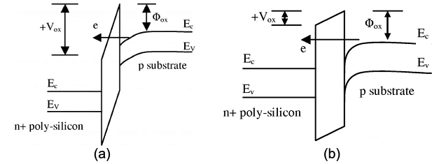
Thin gate oxides provide large electric fields on the SiO layer in short-channel devices. Electrons tunnel from the substrate to the gate and from the gate through the gate oxide to the substrate when the oxide thickness is low and the electric field is high, resulting in gate oxide tunneling current.
Consider the band diagram shown in the figure.

Figure 2. Band Diagram of a MOS Transistor with (a) Flat Band, (b) Positive Gate Voltage, and (c) Negative Gate Voltage
The first figure, Figure 2(a), is a flat-band MOS transistor. i.e. no charge exists in it.
The band diagram changes when the gate terminal is forward biased, as illustrated in the second graph, Figure 2. (b). Gate current is generated when electrons at the strongly inverted surface tunnel into or through the SiO layer.
A negative gate voltage, on the other hand, causes electrons from the n+ polysilicon gate to tunnel into or through the SiO2 layer, producing in a gate current, as shown in Fig. 2. (c).
Fowler-Nordheim tunnel and direct tunnel
There are mainly two tunneling mechanisms between the gate and the substrate. they are:
Fowler-Nordheim tunneling, where electrons tunnel through a triangular barrier
Direct tunneling, where electrons tunnel through a ladder barrier

Figure 3. Band Diagrams Showing (a) Fowler-Nordheim Tunneling through a Triangular Barrier of Oxides and (b) a Ladder Barrier for Direct Tunneling through Oxides
You can see the band diagrams of the two tunneling mechanisms in Figures 3(a) and 3(b) above.
4. Leakage current due to hot carrier injection from the substrate to the gate oxide
The high electric field near the substrate-oxide interface excites electrons or holes, which pass the substrate-oxide interface and into the oxide layer in short-channel devices. Hot carrier injection is the term for this phenomenon.

Figure 4. Band Diagram Depicting Electrons Gaining Sufficient Energy due to High Electric Field to Cross the Oxide Barrier (Hot Carrier Injection Effect)
Electrons are more susceptible to this phenomena than holes. This is due to the fact that electrons have a lower effective mass and a lower barrier height than holes.
5. Leakage current due to gate induced drain drop (GIDL)
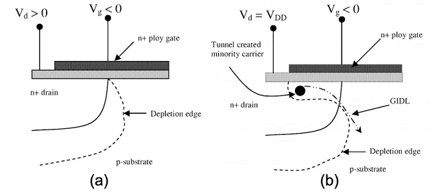
Take an NMOS transistor with a p-type substrate as an example. Positive charge builds exclusively at the oxide-substrate interface when there is a negative voltage at the gate terminal. Due to the holes accumulating on the substrate, the surface behaves as a more strongly doped p-region than the substrate.
As a result, the depletion zone along the drain-substrate contact is thinner near the surface (compared to the thickness of the depletion region in the bulk).

Figure 5. (a) Formation of a Thin Depletion Region Along the Surface at the Drain-Substrate Interface and (b) GIDL Current Flow due to Avalanche Effect and BTBT-Generated Carriers
Avalanche and interband tunneling effects (as discussed in the first part of this study) occur due to the thin depletion area and greater electric field. As a result, minority carriers are created in the drain region under the gate, and the negative gate voltage pushes them into the substrate. Leakage current rises as a result of this.
6. Leakage current due to punch-through effect
Because the drain and source are close together in short-channel devices, the depletion areas of the two terminals converge and eventually overlap. "Penetration" is said to have occurred in this case.
For most carriers from the source, the punch-through effect lowers the barrier. The number of carriers entering the substrate increases as a result of this. The drain collects some of these carriers, while the remainder generate leakage current.

Frequently Asked Questions


