

AD210AN Isolation Amplifier: Pinout, Applications, Datasheet
yunying Release time:2023-09-12 Page View:495
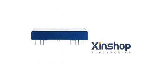
The AD210AN is a Precision, Wide Bandwidth 3-Port Isolation Amplifier. This article will unlock its pinout, datasheet, parts comparison and more details about AD210AN.
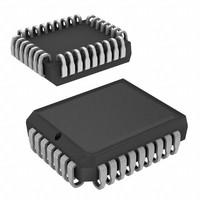
1 Channels 5mA per Channel 30pA 120 dB Instrumentational OP Amps 15V 14.25V~15.75V AD210 12 Pins 38-DIP (0.800, 20.32mm), 12 Leads
AD210AN Pinout
Pin | Designation | Function |
1 | Vo | Output |
2 | Ocom | Output Common |
3 | +VOSS | +Isolated Power @ Output |
4 | –VOSS | -Isolated Power @ Output |
14 | +VISS | +Isolated Power @ Input |
15 | –VISS | -Isolated Power @ Input |
16 | FB | Input Feedback |
17 | –IN | –Input |
18 | Icom . | Input Common |
19 | +IN | +Input |
29 | Pwr Com | Power Common |
30 | Pwr | Power Input |
AD210AN Overview
The AD210AN is the most recent member of a new class of high-quality, affordable isolation amplifiers. This surface-mounted, automated assembly procedure is used to create this three-part, broad bandwidth isolation amplifier. The AD210AN creates a very compact and affordable isolator whose performance and abundance of user features greatly exceed those provided by more expensive devices by combining design experience with cutting-edge manufacturing technology.
AD210AN CAD Model
Symbol

AD210AN Symbol
Footprint

AD210AN Footprint
3D Model

AD210AN Applications
Multichannel Data Acquisition
High Voltage Instrumentation Amplifier
Current Shunt Measurements
Process Signal Isolation
AD210AN Functional Block Diagram
Figure 1 depicts below the AD210AN basic block diagram. A +15 V supply is connected to the power port, and a 50 kHz carrier frequency supplies 15 V isolated power to both the input and output ports. The uncommitted input amplifier can provide gain or buffer to the AD210AN. The full-wave modulator converts the signal to the carrier frequency, which is then applied to transformer T1. The synchronous demodulator reconstructs the input signal in the output port. A 20 kHz three-pole filter is used to reduce output noise and ripple. Finally, an output buffer outputs a low-impedance signal capable of driving a 2 kΩ load.
The fundamental block diagram for the AD210AN is shown below in Figure 1. The power port is connected to a +15 V supply, and the input and output ports receive isolated 15 V power at a carrier frequency of 50 kHz. The uncommitted input amplifier can give the AD210AN gain or a buffer. The signal is changed to the carrier frequency via the full-wave modulator and then applied to transformer T1. The output port of the synchronous demodulator reconstructs the input signal. The output noise and ripple are decreased using a 20 kHz three-pole filter. An output buffer then produces a low-impedance signal that can drive a 2 k load.

Figure1.AD210AN Functional Block Diagram
AD210AN Usages
It is quite easy to use the AD210AN in a multitude of applications. In both single-channel and multichannel systems, the AD210AN, which is powered by a single +15 V power source, excels as an input or output isolator.
Figure 2 shows the fundamental unity gain configuration for signals up to 10 V. Additional types of input amplifiers are shown in the figures below. Figure 3 demonstrates how to maintain a very high input impedance for lower signal levels while achieving gain.

Figure2.Basic Unity Gain Configuration
The circuits in Figures 2 and 3 can maintain their high input impedance in an inverting application. Signal inversion is possible with the AD210AN's three ports by switching the input and output leads.

Figure3.Input Configuration for G
Figure 4 demonstrates how to accept input currents, total currents, or voltages. Signals greater than 10 V can also be used with this circuit arrangement. For instance, RF = 20 k and RS1 = 200 k can withstand a 100 V input span.

Figure4.Summing or Current Input Configuration
AD210AN Dimensions

AD210AN Dimensions
Datasheet PDF
Please swipe to the lasst two part for Downloading AD210AN datasheets, AD210AN specifications and manufacturer documentation.
To use AD210AN well, you should know:
AD210AN technical specifications, attributes, parameters and parts with similar specifications
The AD210AN is a precision, monolithic, low cost, wide bandwidth, internally trimmed, and biFET operational amplifier. Here are some general steps to use the AD210AN in a circuit:
1. **Pin Configuration:** The AD210AN typically comes in an 8-pin DIP (Dual Inline Package) package. Familiarize yourself with the pinout of the device. The pins are usually labeled with numbers and functions such as V+, V-, Output, etc.
2. **Power Supply:** The AD210AN requires power supplies for its operation. Connect the positive (+V) and negative (-V) power supply pins to the appropriate voltage levels as specified in the datasheet. Make sure to adhere to the recommended voltage levels to prevent damage to the device.
3. **Input Signals:** The AD210AN is an operational amplifier, so you typically connect your input signals to the non-inverting and inverting input pins of the amplifier. The non-inverting input is usually denoted as (+) and the inverting input as (-).
4. **Feedback Network:** Operational amplifiers require a feedback network to control the gain and other characteristics of the amplifier. Depending on your circuit requirements, you may need to connect external resistors and capacitors in a feedback configuration.
5. **Output:** The output of the AD210AN is usually taken from the Output pin. This is where the amplified signal is available for further processing in your circuit.
6. **Ground Connections:** Make sure to connect the ground pin of the AD210AN to the common ground of your circuit to ensure proper operation.
7. **Decoupling Capacitors:** It is often good practice to include decoupling capacitors near the power supply pins of the AD210AN to filter out noise and ensure stable operation.
8. **Biasing:** Depending on the specific application, you may need to bias the inputs or outputs of the AD210AN to achieve the desired operating conditions.
Specifications
- Manufacturer :
- Analog Devices, Inc.
- Product Category :
- Instrumentation, OP Amps, Buffer Amps
- -3db Bandwidth :
- 15MHz
- Amplifier Type :
- Isolation
- Bandwidth :
- 20 kHz
- Base Part Number :
- AD210
- Common Mode Rejection Ratio :
- 120 dB
- Common Mode Voltage-Max :
- 3500V
- Current - Input Bias :
- 30pA
- Dual Supply Voltage :
- 15V
- ECCN Code :
- EAR99
- Factory Lead Time :
- 20 Weeks
- Height :
- 8.91mm
- Input Offset Voltage (Vos) :
- 15mV
- Isolation Voltage :
- 15V
- Lead Free :
- Contains Lead
- Length :
- 53.3mm
- Lifecycle Status :
- Production (Last Updated: 1 month ago)
- Moisture Sensitivity Level (MSL) :
- 1 (Unlimited)
- Mount :
- Through Hole
- Mounting Type :
- Through Hole
- Nominal Supply Current :
- 50mA
- Number of Channels :
- 1
- Number of Elements :
- 2
- Number of Functions :
- 1
- Number of Pins :
- 12
- Number of Terminations :
- 12
- Operating Supply Current :
- 50mA
- Operating Supply Voltage :
- 15V
- Operating Temperature :
- -25°C~85°C
- Output Current per Channel :
- 5mA
- Package / Case :
- 38-DIP (0.800, 20.32mm), 12 Leads
- Packaging :
- Tube
- Part Status :
- Active
- Pbfree Code :
- No
- Pin Count :
- 12
- Radiation Hardening :
- No
- REACH SVHC :
- No SVHC
- Resistance :
- 1 TΩ
- RoHS Status :
- Non-RoHS Compliant
- Slew Rate :
- 1V/μs
- Supply Voltage :
- 15V
- Terminal Position :
- Dual
- Termination :
- Through Hole
- Voltage - Supply, Single/Dual (±) :
- 14.25V~15.75V
- Voltage Gain :
- 40dB
- Width :
- 25mm
Datasheets
- Datasheets
- AD210AN
- Share this post
-


Frequently Asked Questions
How does AD210AN work?
Related Articles

DRV8908QPWPRQ1 Motor Driver Datasheet,Pinout,Specification
LIS3DHTR Accelerometer for Your Projects
TMS320F28335PGFA Datasheet, Pinout, Specification
NE555 vs NE5532:Comparison for Electronics Enthusiasts
NE5532 vs OPA1612 Op-Amp: Choosing Your Right One
STM32 STM32G070RBT6 Datasheet for Embedded Systems
ADM2587EBRWZ RS-485/RS-422 Transceiver:Datasheet
CH340 vs CP2102 vs CH341 vs FT232 Differences
LM324 Op amp Pinout,Datasheet,Spec,Circuit:How to Test LM324?
What Is The Difference Between 7812 And 7805?PDF,Price,Pinout


-
1,000+Daily Order Quantity
-
2,500,000+Alternative Parts
-
2,200+Worldwide Manufacturers
-
10,000 ㎡In-stock Warehouse


