Ultimate Tutorial to JTAG: Understanding the Basics and Operation
Dear friends, this article is Ultimate Tutorial to JTAG. In this post you could find frenquently asked questions about JTAG including boundary scan, JTAG Programmer and Debugger, difference between JTAG and UART, and how to implement it.
CATALOG
What is JTAG?
Applications of JTAG
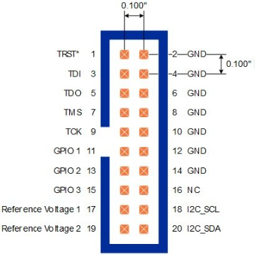
JTAG Pinout
JTAG Protocol and Interface
JTAG Connectors
JTAG Programmer and Debugger
JTAG Software
JTAG on Xbox 360
JTAG test operations
What is Boundary scan?
What is the difference between JTAG and UART?
How to implement a JTAG interface using VHDL on an FPGA?
JTAG, which stands for Joint Test Action Group, is a widely used industry standard for testing and debugging electronic circuits. In this comprehensive tutorial, we will delve into the key aspects of JTAG, including its applications, protocols, connectors, pinouts, programmers, debuggers, and software.
What is JTAG?
JTAG is a standard defined by the IEEE 1149.1 standard for testing and debugging printed circuit boards (PCBs) using a standard set of test points. It enables a variety of functions such as boundary scan testing, in-system programming, and real-time debugging.
Applications of JTAG
- **Testing and Debugging:** JTAG is commonly used for testing connections between integrated circuits on a PCB.
- **Programming:** In-system programming allows for updating firmware or configuration data on devices.
- **Debugging:** JTAG debuggers are utilized for real-time monitoring and troubleshooting of embedded systems.
JTAG Protocol and Interface
The JTAG protocol defines a standard method for testing and debugging digital integrated circuits. It enables communication with devices through a standardized interface, typically using a 4-wire or 5-wire interface.
JTAG pinout scan
We can detect the pinout using a microcontroller like Arduino with specific software for this purpose. There are several implementations, probably JTAGenum is the best one.

JTAG Connectors
JTAG connectors feature a specific pinout arrangement to facilitate communication between the JTAG programmer or debugger and the target device. The standard JTAG connector often includes pins for TCK (Test Clock), TMS (Test Mode Select), TDI (Test Data In), TDO (Test Data Out), and other optional lines.
JTAG Programmer and Debugger
A JTAG programmer is a device used to program firmware or data into a target device, while a JTAG debugger allows for real-time monitoring and debugging of embedded systems. These tools are essential for development and testing processes.
What is a J-Link debugger?
What is the use of JTAG in FPGA programming?
JTAG Software
There are various software tools available for working with JTAG-enabled devices. These tools provide interfaces for programming, debugging, and testing, making it easier to interact with JTAG-compliant hardware.
JTAG on Xbox 360
What does a JTAG kit do for Xbox 360? JTAG on Xbox 360 refers to a method of modifying the console to run unsigned code, homebrew applications, and custom firmware. This process, although popular among enthusiasts, is not endorsed by Microsoft and can void warranties.
What is Boundary scan?
Boundary Scan
The main advantage offered by utilising boundary scan technology is the ability to set and read the values on pins without direct physical access.

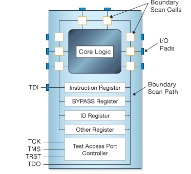
Schematic Diagram of a JTAG enabled device
The process of boundary scan can be most easily understood with reference to the schematic diagram shown in figure 1.
All the signals between the device’s core logic and the pins are intercepted by a serial scan path known as the Boundary Scan Register (BSR) which consists of a number of boundary scan ‘cells’. In normal operation these boundary scan cells are invisible. However, in test mode the cells can be used to set and/or read values from the device pins (or in ‘internal’ mode from values of the core logic.) Not all boundary scan cells are the same – there are 10 types of cell in the 1149.1 standards, though manufacturers can define non-standard cell types to match the actual hardware functionality of their device if they wish.
Interface Signals
The JTAG interface, collectively known as a Test Access Port, or TAP, uses the following signals to support the operation of boundary scan.
· TCK (Test Clock) – this signal synchronizes the internal state machine operations.
· TMS (Test Mode Select) – this signal is sampled at the rising edge of TCK to determine the next state.
· TDI (Test Data In) – this signal represents the data shifted into the device’s test or programming logic. It is sampled at the rising edge of TCK when the internal state machine is in the correct state.
· TDO (Test Data Out) – this signal represents the data shifted out of the device’s test or programming logic and is valid on the falling edge of TCK when the internal state machine is in the correct state.
· TRST (Test Reset) – this is an optional pin which, when available, can reset the TAP controller’s state machine.
Registers
There are two types of registers associated with boundary scan. Each compliant device has one instruction register and two or more data registers.
Instruction Register – the instruction register holds the current instruction. Its content is used by the TAP controller to decide what to do with signals that are received. Most commonly, the content of the instruction register will define to which of the data registers signals should be passed.
Data Registers – there are three primary data registers, the Boundary Scan Register (BSR), the BYPASS register and the IDCODES register. Other data registers may be present, but they are not required as part of the JTAG standard.
· BSR – this is the main testing data register. It is used to move data to and from the I/O pins of a device.
· BYPASS – this is a single-bit register that passes information from TDI to TDO. It allows other devices in a circuit to be tested with minimal overhead.
· IDCODES – this register contains the ID code and revision number for the device. This information allows the device to be linked to its Boundary Scan Description Language (BSDL) file. The file contains details of the Boundary Scan configuration for the device.
Test Access Port (TAP) Controller
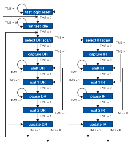
The TAP controller, a state machine whose transitions are controlled by the TMS signal, controls the behaviour of the JTAG system. Figure below, shows the state-transition diagram.

TAP State machine
All states have two exits, so all transitions can be controlled by the single TMS signal sampled on TCK. The two main paths allow for setting or retrieving information from either a data register or the instruction register of the device. The data register operated on (e.g. BSR, IDCODES, BYPASS) depends on the value loaded into the instruction register.
For more detail on each state, refer to the IEEE 1149.1 Standard JTAG document.
Boundary Scan Instructions
The IEEE 1149.1 standard defines a set of instructions that must be available for a device to be considered compliant. These instructions are:
· BYPASS – this instruction causes the TDI and TDO lines to be connected via a single-bit pass-through register (the BYPASS register). This instruction allows the testing of other devices in the JTAG chain without any unnecessary overhead.
· EXTEST – this instruction causes the TDI and TDO to be connected to the Boundary Scan Register (BSR). The device’s pin states are sampled with the ‘capture dr’ JTAG state and new values are shifted into the BSR with the ‘shift dr’ state; these values are then applied to the pins of the device using the ‘update dr’ state.
· SAMPLE/PRELOAD – this instruction causes the TDI and TDO to be connected to the BSR. However, the device is left in its normal functional mode. During this instruction, the BSR can be accessed by a data scan operation to take a sample of the functional data entering and leaving the device. The instruction is also used to preload test data into the BSR prior to loading an EXTEST instruction.
Other commonly available instructions include:
· IDCODE – this instruction causes the TDI and TDO to be connected to the IDCODE register.
· INTEST – this instruction causes the TDI and TDO lines to be connected to the Boundary Scan Register (BSR). While the EXTEST instruction allows the user to set and read pin states, the INTEST instruction relates to the core-logic signals of a device.
What is the difference between JTAG and UART?
JTAG and UART are two different communication interfaces commonly used in embedded systems for different purposes. Here are the key differences between JTAG and UART:
1. **Functionality:**
- **JTAG (Joint Test Action Group):** JTAG is primarily used for testing, debugging, and programming integrated circuits on a PCB. It allows for boundary scanning, debugging of firmware, and programming of flash memory.
- **UART (Universal Asynchronous Receiver-Transmitter):** UART is used for serial communication between devices. It enables the transmission and reception of data between devices in a simple and asynchronous manner.
2. **Interface Type:**
- **JTAG:** JTAG uses a standardized Test Access Port (TAP) controller and a specific set of pins on the target device for communication. It is designed for low-level access to the internal components of a device for testing and debugging purposes.
- **UART:** UART uses two pins (TX and RX) for serial communication. It operates at a specific baud rate and can be used for sending and receiving data in a serial format.
3. **Applications:**
- **JTAG:** JTAG is commonly used in hardware debugging, firmware development, and boundary scan testing. It is often used by hardware engineers and firmware developers for low-level access to the internal components of a device.
- **UART:** UART is used for communication between devices, such as microcontrollers, sensors, and other peripherals. It is commonly used for sending data between devices over a serial connection.
4. **Speed and Efficiency:**
- **JTAG:** JTAG is designed for low-level access and debugging tasks, which can make it more efficient for tasks like boundary scan testing and programming flash memory.
- **UART:** UART is more suitable for serial data transmission between devices at a moderate speed. It is commonly used for sending data between devices in real-time communication scenarios.
How to implement a JTAG interface using VHDL on an FPGA?
Design the TAP Controller: The Test Access Port (TAP) controller is the core component of the JTAG interface. It manages the JTAG state machine and controls the data transfer between the FPGA and external devices. The TAP controller typically includes state registers, shift registers, and control logic.
Design the Instruction Register: The Instruction Register (IR) stores the instruction data during the JTAG operation. It is used to select the operation to be performed, such as shifting in data or selecting a specific boundary scan register.
Design the Data Register: The Data Register (DR) stores the data that is shifted in or out during JTAG operations. It is used for transferring test data, configuration data, or other information between the FPGA and external devices.
Implement the JTAG State Machine: The JTAG state machine defines the different states of the JTAG operation, such as Test-Logic-Reset (TLR), Run-Test/Idle (RTI), Shift-IR, Shift-DR, and others. The state machine transitions between these states based on control signals and input data.
Implement Boundary Scan Cells: If you are using JTAG for boundary scan testing, you will need to implement boundary scan cells in your design. These cells allow you to test the interconnections between components on the FPGA.
Write VHDL Code for the JTAG Interface: Write VHDL code for the TAP controller, IR, DR, JTAG state machine, and any other necessary components. Ensure that the code is compliant with the JTAG standard and follows the required protocol for communication.
Test and Verify the JTAG Interface: Once you have implemented the JTAG interface in VHDL, test it thoroughly to ensure that it functions correctly. Test different JTAG operations, boundary scan testing, and data transfer to verify the functionality of the interface.
In conclusion, JTAG is a versatile standard that plays a crucial role in testing, programming, and debugging electronic circuits. By understanding the fundamentals of JTAG and its various applications, developers and engineers can leverage its capabilities to streamline the development and testing processes of electronic systems.
What is a JTAG debugger?
How to connect a JTAG debugger to your microcontroller?

Frequently Asked Questions


