SS8050 NPN Epitaxial Silicon Transistor: Equivalent, Pinout, Datasheet
![bc11fc1318be920c94f3f5e92a875c34.png 5NZC_~D$QDLVPI_]@%8`O43](/upload/image/content/20231009/bc11fc1318be920c94f3f5e92a875c34.png)
SS8050 NPN Epitaxial Silicon Transistor
Catalog
SS8050 Description
SS8050 Pinout
SS8050 CAD Model
SS8050 Features
SS8050 Applications
SS8050 Alternatives
SS8050 Typical Application Circuit
SS8050 Functional Block Diagram
SS8050 Package
Datasheet PDF
Specifications
Product comparison
SS8050 Description
Because the SS8050 is an NPN transistor, the collector and emitter will be open (reverse biased) when the base pin is held at ground and closed (forward biased) when a signal is applied to the base pin. It has a maximum gain of 400, which specifies the amplification capability of the transistor, which is generally SS8050. Because it is so high, it is typically utilized for amplification. However, the typical value of gain for a normal running collector current is 110. Because the maximum amount of current that may flow through the Collector pin is 700mA, we cannot use this transistor to drive loads that consume more than 700mA. To bias a transistor, we must feed current to the base pin; this current (IB) should be kept to a maximum of 5mA.
When fully biased, this transistor can enable a maximum of 700mA to pass across the collector and emitter. This is known as the Saturation Region, and the typical voltage allowed across the Collector-Emitter (VCE) or Collector-Base (VCB) could be 20V or 30V. When the base current is eliminated, the transistor turns completely off; this is referred to as the Cut-off Region.
To bias a transistor, we must feed current to the base pin; this current (IB) should be kept to a maximum of 5mA.
When fully biased, this transistor can enable a maximum of 700mA to pass across the collector and emitter.
This is known as the Saturation Region, and the typical voltage allowed across the Collector-Emitter (VCE)
or Collector-Base (VCB) could be 20V or 30V. When the base current is eliminated, the transistor turns
completely off; this is referred to as the Cut-off Region.
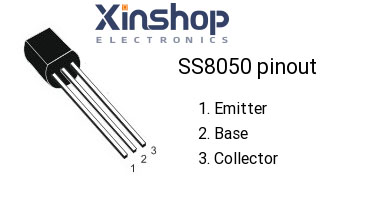
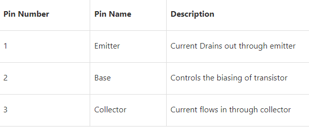
SS8050 Pinout
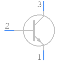
SS8050 CAD Model
Symbol
Footprint

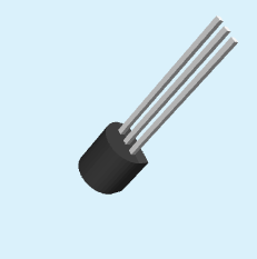
3D-model
SS8050 Features
●2 W Output Amplfer of Portable Radios in Class B Push-pull Operation.
●Complimentary to SS8550
●Collector Current: lc= 1.5 A
SS8050 Applications
Audio Amplification Circuits
Class B Amplifiers
Push pull Transistors
Circuits where high gain is required
Low signal applications
SS8050 Alternatives
SS8050 Application Circuit
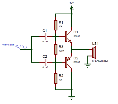
SS8050 Functional Block Diagram
SS8050 Dimension
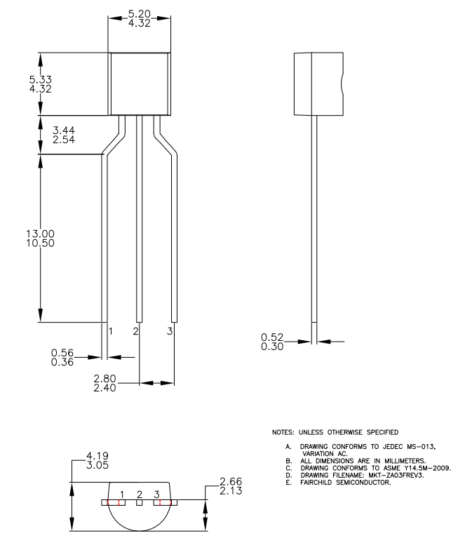
SS8050 Package
Datasheet PDF
Please DOWNLOAD the datasheets and manufacturer documentation for the SS8050.
Specifications
Product comparison


