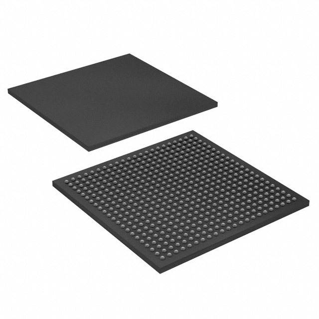
EP3C55F484I7N Vs EP3C40F484C8N FPGA Comparison: Datasheet, Features
This post is about the Comparative Analysis of EP3C55F484I7N and EP3C40F484C8N

In the high-performance FPGA (Field-Programmable Gate Array) market, Altera's (now acquired by Intel and renamed Intel PSG) EP3C series has been attracting a lot of attention for its high performance and low power consumption. Today, we will compare and analyze two FPGAs, EP3C55F484I7N and EP3C40F484C8N.
Wait, what? What are FPGAs? FPGAs are programmable integrated circuits that can be customized to perform specific functions by configuring the internal logic elements and interconnections. They are commonly used in fields such as telecommunications, automotive, aerospace, and industrial automation, where flexibility and reconfigurability are important.
EP3C55F484I7N and EP3C40F484C8N are both part numbers for specific FPGAs (Field-Programmable Gate Arrays) manufactured by Altera, which is now a part of Intel.
What is EP3C55F484I7N ?

The EP3C55F484I7N is a member of the Cyclone III FPGA family. It has 55,000 logic elements (LEs) and comes in a 484-pin FineLine BGA (Ball Grid Array) package with an industrial temperature range. The "I7" in the part number represents the speed grade of the FPGA.
What is EP3C40F484C8N ?

The EP3C40F484C8N is also part of the Cyclone III FPGA family. It has 40,000 logic elements (LEs) and comes in a 484-pin FineLine BGA package with a commercial temperature range. The "C8" in the part number represents the speed grade of the FPGA.
Features
Lowest Power FPGAs
■ Lowest power consumption due to:
■ TSMC low-power process technology
■ Altera® power-aware design flow
■ Low-power operation offers the following benefits:
■ Extended battery life for portable and handheld applications
■ Reduced or eliminated cooling system costs
■ Operation in thermally-challenged environments
■ Hot-socketing operation support
Design Security Feature
Cyclone III LS devices offer the following design security features:
■ Configuration security using advanced encryption standard (AES) with 256-bit
volatile key
■ Routing architecture optimized for design separation flow with the Quartus® II
software
■ Design separation flow achieves both physical and functional isolation
between design partitions
■ Ability to disable external JTAG port
■ Error Detection (ED) Cycle Indicator to core
■ Provides a pass or fail indicator at every ED cycle
■ Provides visibility over intentional or unintentional change of configuration
random access memory (CRAM) bits
■ Ability to clear contents of the FPGA logic, CRAM, embedded memory, and
AES key
■ Internal oscillator enables system monitor and health check capabilities
First, specifically, let's take a look at the basic specifications of these two FPGAs. The EP3C55F484I7N has 55K logic cells, while the EP3C40F484C8N has 40K logic cells. In digital signal processing and parallel processing-intensive applications, more logic cells mean more processing power. Therefore, from this perspective, the EP3C55F484I7N has an advantage in processing power.
Next, let's look at the memory resources of the two FPGAs. the EP3C55F484I7N provides 1.1MB of RAM resources, while the EP3C40F484C8N provides 1MB of RAM resources. Although the difference is small, the EP3C55F484I7N still has a slight advantage.
Moving on to clock resources, the EP3C55F484I7N provides 16 clock managers while the EP3C40F484C8N provides 12 clock managers. The clock managers can be used to implement more complex timing designs, so the EP3C55F484I7N may be better suited in applications where fine control of the clock is required.
However, in terms of the number of I/O units, the EP3C40F484C8N significantly exceeds the EP3C55F484I7N's 160 with 220. This means that the EP3C40F484C8N may have better performance in applications that require a large number of I/O interfaces, such as serial communications, video interfaces, and so on.
In addition, both FPGAs support a variety of protocols, including PCI Express, RapidIO, Gigabit Ethernet, and more. However, the EP3C55F484I7N supports the 10GBASE-KR interface, which is not available in the EP3C40F484C8N. This feature gives the EP3C55F484I7N a greater advantage in high-speed network applications.
EP3C55F484I7N and EP3C40F484C8N, Which is better?
Overall, the EP3C55F484I7N and EP3C40F484C8N are both excellent FPGAs, each with its own advantages in different application areas. In projects that require more processing power and memory resources, the EP3C55F484I7N may be more suitable. And in projects that require a large number of I/O interfaces or specific high-speed network interfaces, the EP3C40F484C8N may be superior. Therefore, when selecting these two FPGAs, the decision needs to be based on the actual application requirements.

Frequently Asked Questions


